E-Beam Lithography: Precision in Microfabrication
Electron-beam lithography (e-beam lithography) stands out as a critical technique in the field of microfabrication. This method employs a focused beam of electrons to create intricate patterns on a substrate, crucial for producing high-resolution features in semiconductor devices, microelectromechanical systems (MEMS), and nanostructures.
 Discheminc
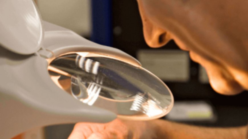
Electron-beam lithography (e-beam lithography) stands out as a critical technique in the field of microfabrication. This method employs a focused beam of electrons to create intricate patterns on a substrate, crucial for producing high-resolution features in semiconductor devices, microelectromechanical systems (MEMS), and nanostructures. Unlike traditional photolithography, which uses ultraviolet light, e-beam lithography offers much finer resolution, making it ideal for applications where precision is paramount.
The process begins with a substrate coated with an electron-sensitive resist material. The e-beam exposes specific areas of this resist, causing chemical changes that allow for selective etching. This technique is known for its ability to produce patterns with nanometer precision, which is essential for developing advanced electronic components and research devices. By controlling the exposure and development processes, manufacturers can achieve highly detailed and accurate features that are crucial for cutting-edge technologies.
The Role of E-Beam Lithography in Modern Fabrication
E-beam lithography is particularly useful in research and development environments where custom, high-precision patterns are required. Its high resolution makes it indispensable for applications in fields such as nanoelectronics, optoelectronics, and photonics. Researchers and engineers rely on this technology to create features at scales that are beyond the reach of traditional photolithography methods.
In semiconductor fabrication, for example, e-beam lithography enables the production of complex patterns on silicon wafers used in microchips. This precision is critical for the development of high-performance devices with densely packed transistors and intricate circuit designs. Similarly, in the field of MEMS, e-beam lithography allows for the creation of microscale mechanical structures and sensors that are integral to many modern devices.
Advantages of E-Beam Lithography
E-beam lithography offers several key advantages over other lithographic methods. First and foremost, its ability to achieve extremely fine resolution is unmatched, allowing for the creation of intricate patterns that are essential for advanced technology applications. Additionally, e-beam lithography does not require masks, which simplifies the process of pattern design and reduces costs associated with mask production.
Another significant benefit is the flexibility it provides in patterning. Researchers can quickly adjust and customize patterns, making e-beam lithography ideal for prototyping and experimental work. This adaptability accelerates the development cycle and allows for rapid iteration and testing of new designs.
Dischem's Sulfamate Nickel Plating Solution: A Complement to E-Beam Lithography
In conjunction with e-beam lithography, Dischem’s sulfamate nickel plating solution plays a crucial role in ensuring the quality and functionality of microfabricated components. This plating solution is specifically designed to meet the demanding requirements of microlithography applications. The high-purity nickel deposits provided by this solution contribute to the durability and performance of the finished products.
Dischem’s sulfamate nickel plating solution features an exceptional nickel metal concentration and low levels of impurities, which enhances the quality of the electroformed components. This results in a smoother surface finish and reduced defects, such as nodules or increased grain size, which are critical factors in maintaining high standards in microfabrication.
Final Remarks
E-beam lithography remains a vital technology in the field of microfabrication, offering unmatched precision and flexibility for creating intricate patterns at the nanometer scale. Its applications span various industries, from semiconductor manufacturing to research and development in advanced technologies. Complementing this technology with Dischem’s sulfamate nickel plating solution ensures that the components produced meet the highest standards of quality and performance. By addressing both the patterning and finishing aspects of microfabrication, Dischem helps enhance the overall reliability and effectiveness of your fabrication processes.