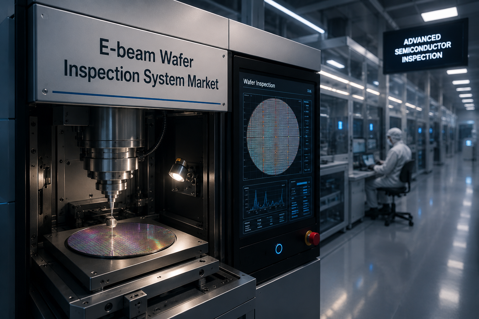
Why the E Beam Wafer Inspection System Market Is Becoming Critical for Advanced Node Manufacturing
The E-beam Wafer Inspection System Market size is expected to reach US$ 3.77 Billion by 2034 from US$ 1.06 Billion in 2025. The market is estimated to record a CAGR of 17.15% from 2026 to 2034.
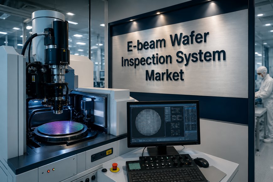
E beam wafer inspection systems deliver high resolution imaging that enables comprehensive inspection of semiconductor wafers throughout the manufacturing cycle. This technology helps manufacturers minimize defects while ensuring consistent production quality.
E Beam Wafer Inspection System Market Overview
According to The Insight Partners, the E Beam Wafer Inspection System Market is expected to grow from US$ 1.06 billion in 2025 to US$ 3.77 billion by 2034, registering a CAGR of 17.15% during the forecast period from 2026 to 2034. The increasing demand for advanced semiconductor devices, continuous technology scaling, growing adoption of artificial intelligence, high-performance computing, and expanding investments in semiconductor manufacturing facilities are driving the growth of the industry.
E Beam Wafer Inspection System Market Analysis: Growth Drivers and Opportunities
The E Beam Wafer Inspection System Market is experiencing rapid expansion due to increasing complexity in semiconductor manufacturing processes. As integrated circuits continue to evolve with smaller geometries and higher transistor densities, manufacturers require inspection technologies capable of identifying microscopic defects with exceptional precision.
The rapid growth of artificial intelligence, cloud computing, automotive electronics, 5G infrastructure, and consumer electronics has accelerated global semiconductor production. This trend has significantly increased demand for advanced wafer inspection equipment capable of supporting higher manufacturing yields and improved product reliability. Additionally, government investments in domestic semiconductor manufacturing and expanding fabrication capacity worldwide continue to create substantial opportunities for equipment manufacturers.
Get a Sample PDF Report: https://www.theinsightpartners.com/sample/TIPRE00021728
Market Segmentation Analysis
The E Beam Wafer Inspection System Market is segmented across multiple categories to provide a detailed understanding of current industry dynamics.
By Type
- Single Beam Inspection System
- Multi Beam Inspection System
By Application
- Integrated Device Manufacturers (IDMs)
- Foundries
- Research Institutes
- Others
The multi beam inspection segment continues to gain traction due to its ability to deliver higher throughput while maintaining exceptional defect detection accuracy. Foundries and integrated device manufacturers remain the largest adopters as they continue investing in advanced semiconductor process technologies.
Regional Analysis
The report evaluates the E Beam Wafer Inspection System Market across North America, Europe, Asia Pacific, Middle East & Africa, and South & Central America.
Asia Pacific continues to dominate the industry owing to the presence of major semiconductor manufacturing hubs in Taiwan, South Korea, China, and Japan. Significant investments in wafer fabrication facilities and government initiatives supporting semiconductor self-sufficiency continue to drive regional demand.
North America remains an important contributor due to technological innovation, research and development activities, and expansion of semiconductor manufacturing capabilities. Europe is also witnessing increasing investments in advanced semiconductor technologies, while the Middle East & Africa and South & Central America are gradually adopting semiconductor manufacturing technologies through strategic infrastructure investments.
Recent Developments and Technology Trends
Continuous innovation in semiconductor manufacturing is driving technological advancements across the E Beam Wafer Inspection System Market. Manufacturers are introducing next-generation inspection platforms capable of higher throughput, enhanced imaging resolution, artificial intelligence-assisted defect classification, and automated process optimization.
The integration of machine learning algorithms with inspection software enables faster defect identification while improving manufacturing efficiency. Increasing adoption of advanced packaging technologies, chiplet architectures, and extreme ultraviolet (EUV) lithography further strengthens demand for high-performance inspection systems capable of supporting future semiconductor manufacturing requirements.
Competitive Landscape
Competition within the E Beam Wafer Inspection System Market remains highly dynamic as leading manufacturers focus on technological innovation, strategic collaborations, product development, and expanding global manufacturing capabilities. Companies continue investing in research and development to improve inspection speed, defect detection sensitivity, software intelligence, and automation capabilities.
Growing demand for advanced semiconductor devices is encouraging industry participants to develop highly scalable inspection platforms capable of supporting next-generation chip manufacturing technologies.
Key Companies in the E Beam Wafer Inspection System Market
Major companies profiled in the report include:
- KLA Corporation
- Applied Materials Inc.
- Hitachi High-Tech Corporation
- ASML Holding NV
- Lasertec Corporation
- Thermo Fisher Scientific Inc.
- Advantest Corporation
- Camtek Ltd.
- Onto Innovation Inc.
- JEOL Ltd.
Future Outlook
The E Beam Wafer Inspection System Market is expected to witness sustained growth throughout the forecast period as semiconductor manufacturers continue transitioning toward smaller process nodes and more advanced chip architectures. Increasing investments in artificial intelligence, high-performance computing, automotive semiconductors, and advanced packaging technologies will continue driving demand for highly accurate inspection solutions.
The integration of artificial intelligence, machine learning, automation, and advanced imaging technologies will further improve inspection capabilities while reducing manufacturing costs and enhancing production efficiency. Continued expansion of semiconductor fabrication facilities across multiple regions is expected to create long-term opportunities for technology providers operating within the global E Beam Wafer Inspection System Market.
Related Market Research Reports
Chillers Market Size, Share, Growth & Scope Analysis 2030
Distributed Antenna System (DAS) Market Insights & Growth Scope by 2031
About The Partners
The Insight Partners is a Insight global leader in market research, delivering comprehensive analysis and actionable insights across diverse industries. The company empowers decision-makers with data-driven intelligence to navigate evolving markets and accelerate growth.
Contact Us:
- Contact Person: Ankit Mathur
- E-mail: ankit.mathur@theinsightpartners.com
- Phone: +1-646-491-9876